Silicon Photonics for Optical Quantum Technologies
 Jeremy O’Brien
[This is an invited article based on recent works of the authors. -- 2Physics.com]
Authors: Jeremy O’Brien and Alberto Politi
Affiliation: Centre for Quantum Photonics, Department of Physics and Department of Electrical & Electronic Engineering, University of Bristol
Quantum information science has shown that quantum mechanical effects can dramatically improve performance for certain tasks in communication, computation and measurement. Single particles of light – photons – are an excellent choice for quantum technologies because they are relatively noise free; information can be moved around quickly – at the speed of light; and manipulating single photons is easy. For these reasons photons have been widely used in quantum communication, quantum metrology, and quantum lithography settings, as well as quantum bits (or qubits) for quantum information processing [1].
The fact that photons see low noise during the propagation is a great advantage, but, at the same time, makes two photons interact with a negligible probability. Two photons interaction is a fundamental task for quantum information processing, and it is at the heart of the Controlled-NOT (CNOT) gate –one of the building block of a future quantum computer. A 2 photon CNOT gate was demonstrated experimentally back in 2003 [2].
A conspicuous number of different experimental realizations of this CNOT gate have since been developed in recent years by different groups, but all the realizations performed so far are based on bulk optical elements on an optical table and photon propagation in air. This approach is useful for proof of principle quantum logic operation, however, photonic quantum technologies will require scalable, miniaturized gates, with improved performances.
The Team at Bristol University has designed and measured integrated optical devices on a chip, with dimensions measured in millimetres [3]. This impressive miniaturisation was permitted thanks to the silica-on-silicon technology used in commercial devices for modern optical telecommunications, which guides light on a chip in the same way as in optical fibers.
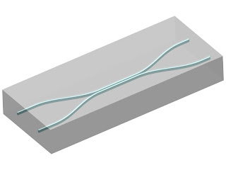
For the first time, the feasibility of integrated quantum information was demonstrated, by achieving the key element of all quantum optics experiments, namely non-classical interference. This effect appears when two indistinguishable photons arrive at the different inputs of a beam-splitter (a half refractive mirror) at the same time. In this case, contrary to the classical analysis, the two photons always exit together from one of the two ports, and they never exit different outputs. The simplest integrated analogous of a free space bream-splitter is a directional coupler, (illustrated in Figure 1). When two waveguides are close one to each other there is a non-zero overlap between the modes of the waveguides. By choosing the waveguide separation and the length of the coupling region, it is possible to choose the amount of power that goes to one waveguide to the other (coupling ratio).
 Figure 1 shows a directional coupler on a chip, the integrated analogue of a beam splitter.
Sending pairs of single photons in the two inputs of the directional coupler, it was possible to demonstrate the quantum interference effect, with a very high visibility of the quantum behaviour.
Using the same technology and various directional couplers with different coupling ratios it is possible to realise a CNOT gate, schematically represented in Figure 1. With this scheme it was possible to achieve a fidelity of the CNOT operation of more than 94%.
 Figure 2 shows the schematic representation of an integrated CNOT gate. The “1/2” and “1/3” numbers indicate the coupling ratio of the different couplers that compose the CNOT gate.
The experimental characterisation of the quantum chips also proved that one of the strangest phenomena of the quantum world, namely “quantum entanglement”, was achieved on-chip. Quantum entanglement of two particles means that the state of either of the particles is not defined, but only their collective state.
This on-chip entanglement has important applications in quantum metrology. Last year Dr O’Brien and his collaborator Professor Takeuchi and co-workers at Hokkaido University reported such a quantum metrology measurement with four photons [4].
The results achieved using integrated chips show that it is possible to realize sophisticated photonic quantum circuits on a silicon chip, which will be of benefit to future quantum technologies based on photons as well as the next generation of fundamental studies in quantum optics.
References
[1] “Optical Quantum Computing”
Jeremy L. O’Brien,
Science 318, 1567 (2007), Abstract.
[2] “Demonstration of an all-optical quantum controlled-NOT gate”
J. L. O'Brien, G. J. Pryde, A. G. White, T. C. Ralph, D. Branning,
Nature 426, 264 (2003), Abstract.
[3] “Silica-on-Silicon Waveguide Quantum Circuits”
A. Politi, M. J. Cryan, J. G. Rarity, S. Yu, J. L. O'Brien,
Science, Vol. 320. no. 5876, pp. 646 - 649 (May 2, 2008)
Published Online March 27, 2008 (10.1126/science.1155441)
Abstract, Link to Full text in the website of Bristol Centre for Quantum Photonics.
[4] "Beating the Standard Quantum Limit with Four-Entangled Photons"
T. Nagata, R. Okamoto, J. L. O'Brien, K. Sasaki, S. Takeuchi,
Science 316, 726 (2007), Abstract.
Labels: Laser 2, Quantum, Quantum Computation and Communication

0 Comments:
Post a Comment